From Feature-Scale Simulation To Digital Twins: Helping Process Engineers Tackle Growing Complexity
Original reporting by Semiconductor Engineering
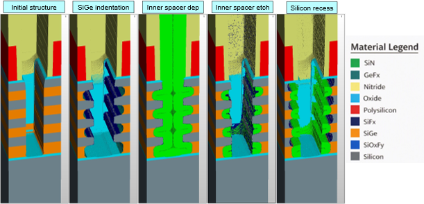
Physics-based simulation in semiconductor manufacturing refers to the use of computational models that apply fundamental physical laws to predict and understand feature-scale wafer outcomes. The relentless march of semiconductor manufacturing toward atomic-scale precision, especially in complex etch processes for advanced nodes, has compounded challenges beyond the capacity of traditional trial-and-error methods. Engineers grapple with an explosion of process parameters, tightening windows, and critical feature-scale effects that directly impact device performance, making a deep, mechanistic understanding indispensable. Physics-based simulation provides this crucial foundation, translating equipment settings and process conditions into predictable wafer-level results by modeling intricate plasma-surface interactions and transport effects in 3D structures.
Beyond raw data This foundational understanding is what truly unlocks the potential of advanced technologies. While AI, automation, and digital twins promise faster exploration and optimization, their power is only fully realized when built upon calibrated, physics-grounded models. Without this physical anchor, AI-driven insights risk being mere data-fitting, unable to generalize or guide true innovation. By establishing a trusted framework that clarifies *why* outcomes occur, physics-based simulation empowers engineers to explore virtual scenarios, accelerate model development, and make credible, data-driven decisions at the speed demanded by modern semiconductor complexity.
The escalating complexity of semiconductor manufacturing irrevocably demands a sophisticated approach where physics-based simulation forms the indispensable foundation. This article has detailed how, in an era of unprecedented process challenges and atomic-scale requirements, mechanistic understanding is not merely advantageous but essential. While AI, automation, and digital twins promise powerful acceleration, their true value and trustworthiness are realized only when anchored by the rigorous, calibrated insights that physics-based models provide. This synergy ensures that exploration is both rapid and reliable, preventing purely empirical approaches from faltering in the face of novel or sparse data scenarios. This integration of fundamental science with advanced computational methods is the key to maintaining process control and predictability as fabrication pushes ever finer limits.
Empowering Future Innovation
This paradigm shift marks a critical evolution in process development, moving beyond the limits of traditional wafer-based experimentation. By integrating physics at the core of AI-driven digital twin workflows, engineers are empowered to explore an exponentially larger solution space with unprecedented confidence, transforming their ability to predict outcomes, troubleshoot issues, and optimize complex steps. The broader implication is not just faster iteration cycles, but deeper, actionable insight into the fundamental behaviors of semiconductor processes. This enhanced capability directly addresses the bottleneck of human capacity in a rapidly expanding innovation space. Ultimately, this integrated strategy will accelerate the development and high-yield production of next-generation devices, ensuring that human ingenuity, amplified by robust physics-based tools and intelligent assistants, continues to drive the industry forward. It positions the industry to consistently meet future demands for performance, power, and cost, solidifying its competitive edge globally.
Frequently asked questions
- Why is physics-based simulation essential for modern semiconductor manufacturing?
- Physics-based simulation provides a mechanistic understanding of complex processes, translating equipment inputs and fab observations into feature-level wafer outcomes. It models plasma-surface interactions and profile evolution, crucial for advanced nodes with atomic-scale requirements. This foundation enables engineers to understand the "why" behind process behaviors and predict results accurately, significantly reducing reliance on costly and time-consuming physical trial-and-error experimentation in fabrication facilities.
- What are the key challenges posed by increasing complexity in semiconductor manufacturing?
- Modern semiconductor manufacturing faces challenges from advanced nodes with tighter atomic-scale requirements, new materials, and narrower process windows. Feature-scale effects directly determine critical dimensions and device performance. This growing complexity makes traditional trial-and-error experimentation too slow and costly, as the number of process interactions and potential solutions outpaces human expert capacity and traditional methods, creating bottlenecks in innovation.
- What role do AI and digital twins play in semiconductor process development?
- AI and digital twins enhance semiconductor process development by building upon physics-based simulations. Digital twins integrate simulation, equipment data, and process knowledge into a unified environment for virtual exploration and decision-making. AI accelerates calibration, optimizes parameters, and searches complex solution spaces. Together, they enable faster exploration, automate repetitive workflows, and facilitate more efficient understanding of process behaviors, helping engineers manage increasing manufacturing complexity effectively.